For decades, the progress of electronics has followed a simple rule: the smaller, the better. Since the 1960s, each new generation of chips has packed more transistors into less space, abiding by Moore’s famous law. Formulated by Intel co-founder Gordon Moore in 1965, this law predicted that the number of components in a microchip would roughly double every year. But that race towards smallness is reaching its physical limit. Now, an international team of scientists proposes a solution that is as obvious as it is revolutionary: if we can’t keep reducing the size of chips, let’s build.
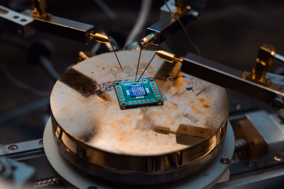
Xiaohang Li, a researcher at King Abdullah University of Science and Technology (KAUST) in Saudi Arabia, and his team have designed a chip with 41 vertical layers of semiconductor and insulation materials, about ten times taller than anything previously produced. The work, recently published in the magazine Nature electronicsit not only represents a technical milestone, but opens the door to a new generation of flexible, efficient and sustainable electronic devices.
“Having six or more layers of transistors stacked vertically allows us to increase the circuit density without shrinking the devices laterally,” Li explains. “With six layers we can integrate 600% more logic functions in the same area than with a single layer, achieving higher performance and lower power consumption.”
Moore’s Law began to lose value around 2010, as chipmakers ran afoul of the laws of physics. Current transistors are only a few nanometers wide, so small that quantum effects are starting to interfere with their operation. “Moore’s law is reaching its physical limits in traditional silicon microelectronics, but innovation continues in new directions. Instead of continuing to reduce the size of transistors, we are exploring new materials, new architectures, and new possibilities, such as stacking,” says Li.
Transistor skyscraper
To understand the technical challenge faced by his team, Li turns to an architectural metaphor: “Think of each layer of transistors as the floor of a skyscraper. If one floor is uneven, the entire building becomes unstable.” The key to the experiment’s success was mastering what they call “interface roughness”: any small imperfection between the layers can interrupt the flow of electrons and drastically reduce the chip’s performance.
The fundamental turning point was the development of completely new production strategies. A crucial point was to have all the layers deposited at or near room temperature, thus protecting the lower layers already made. This low-temperature production is not a simple technical detail. “Most flexible or organic materials cannot withstand high temperatures,” Li explains. “Traditional semiconductor processes often exceed 400°C, which would melt or deform these materials,” he adds. Keeping the entire process at room temperature allows the use of plastic or polymer substrates, opening the door to the flexible electronics of the future.
To demonstrate the feasibility of their design, the team produced 600 copies of the chip, all with similar performance. The researchers used these stacked chips to implement basic operations, achieving performance comparable to traditional non-stacked chips but with much lower power consumption: just 0.47 microwatts, compared to the 210 typical of next-generation devices.
First applications
Where will we first see this technology? Li is optimistic, but realistic: “The first applications will likely be wearable health sensors, smart labels and flexible displays, where low power and mechanical flexibility are crucial.” Longer term, the team envisions large-area computing surfaces, essentially “electronic skins” that can sense, process and communicate across objects or entire structures. While these new chips likely won’t power supercomputers, their use in devices like household appliances could significantly reduce the electronics industry’s carbon footprint.
“The circuits we develop are designed for these systems, where mechanical flexibility, low cost and scalability matter more than extreme speed,” Li clarifies. The researcher believes that his research opens a new door in the field of computing: “It demonstrates that performance scaling can continue, not only by making devices smaller, but by integrating them more intelligently and efficiently in three dimensions.”